Hello,
Please I need your advices,
I am trying to define one sram Model just for simulation with VERILOG:
CYPRESS CY62167EV30 MoBL 16 MBit(1M x 16)32 Byte = 2^4 x 16 bits in
order to test the sram controller.
So I did this:
module ram(Address,Clk,CS,ME,WE,Dout);
input[3:0] Address;
input Clk;
input CS;
input ME;
input WE;
inout[15:0] Dout;
// ----------------------------------------------------------
reg[15:0] memory[15:0]; // Memory block 32Bytes = 16x 2 x 8 Bits = 2^4 x
16 Bits
reg[15:0] Data_Read;
assign Dout=Data_Read;
// Memory Write Block
integer i;
parameter init="";
initial
begin
if(init=="file")
$readmemb("init.dat", memory);
else begin
if(init=="address") begin
for(i=0;i<=15;i=i+1)
memory[i]=i;
end
else begin
if(init=="random") begin
for(i=0;i<=15;i=i+1)
memory[i]= $random;
end
else begin
if(init=="zero") begin
for(i=0;i<=15;i=i+1)
memory[i]=0;
end
else begin
if(init=="x") begin
for(i=0;i<=15;i=i+1)
memory[i]=1'bx;
end
else begin
$display("Error: Incorrect parameter init=%s",init);
$stop;
end
end
end
end
end
end
always@(posedge Clk) begin
if(CS==1) begin
if(WE==1) begin
Data_Read<=16'bz;
//Write in the memory
memory[Address]<=Dout;
end
else begin
if(ME==1)
//Read from the memory
Data_Read<=memory[Address];
end
end
else Data_Read<=16'bz;
end
endmodule
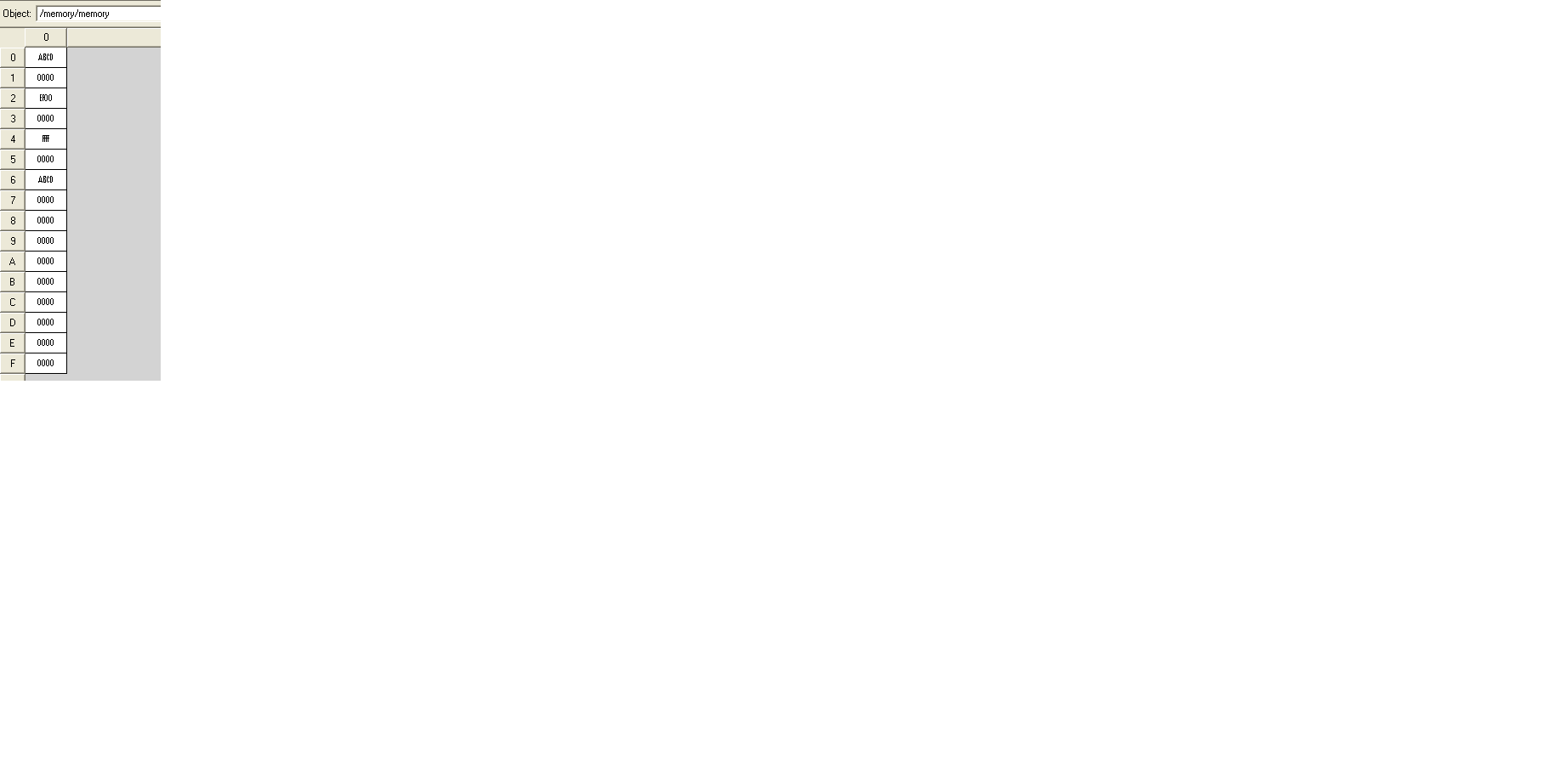
After simulation I realise that my memory has 16 bits word for that
there is one Adress for each 16 bits see the attached files
So what I am doing wrong in order to get one address for each 8 Bits?
and when i tried this reg[7:0] memory[31:0] it didn't match to my Data
bus ?
Angehängte Dateien:
-

Memory_Output.PNG
3,1 KB
You have a 16 bit bus and defined a 16 bit wide register. If you want
both 8 and 16 bit access, then you either need one more address bit or
two byte enables, like most (all?) 16 bit wide SRAMs have.
with two byte enables you can then select witch portion of the bus you
want to aceess:
1 | wire [15:0] memory_word; |
2 | assign memory_word = memory[address]; // Workaround |
3 | |
4 | always@(posedge Clk) |
5 | begin
|
6 | if (CS==1) |
7 | begin
|
8 | if(WE==1) |
9 | begin
|
10 | Data_Read <= 16'hzz; |
11 | //Write in the memory |
12 | if (low_byte == 1'b1) |
13 | memory[Address] <= { memory_word[15:8], Dout[7:0] }; |
14 | if (high_byte == 1'b1) |
15 | memory[Address][15:8] <= { Dout[15:8], memory_word[7:0]}; |
16 | end
|
17 | else
|
18 | begin
|
19 | if(ME==1) |
20 | //Read from the memory |
21 | if (low_byte == 1'b1) |
22 | Data_Read[7:0] <= memory_word[Address][7:0]; |
23 | if (high_byte == 1'b1) |
24 | Data_Read[15:8] <= memory_word[Address][15:8]; |
25 | end
|
26 | end
|
27 | else Data_Read<=16'bz; |
28 | end
|
Dann when you pull both low_byte and high_byte high you can access the
full 16 bit...
Note: No idea if such a workaround works for writting... for reading
should it work.
Thanks,

but in my case, I need to pull my 2 byte Enable to zero because I have a
direct access with 16 bits.
So my concern is doing so I don't get one adress for each byte instead I
have one adress for 16 bits(2 Bytes).
Take a look at the grafic I send in my first mail.
If you only want byte access to the memory then make a model with only
byte access! If you tie the /BYTE input (of the cypress SRAM) to GND,
then you get your extra address line (A0) and only use IO0 to IO7...
(Wild guess follows...) Maybe you want a model that performs both as a
16 and 8 bit memory ?... than you have to add another if to the model
above... (code not tested...)

Note... if the inputs react to HIGH or LOW is not really an issue...
because you can change it in the code!

expand address to 5 bits...
1 | wire [15:0] memory_word; |
2 | assign memory_word = memory[address[4:1]]; // Workaround |
3 | |
4 | always@(posedge Clk) |
5 | begin
|
6 | if (CS == 1'b0) // active low |
7 | begin
|
8 | if (WE == 1'b0) // active low |
9 | begin
|
10 | Data_Read <= 16'hzz; |
11 | if (BYTE == 1'b0) // active low, byte access, extra address line address[0] used! |
12 | if (address[0] == 1'b0) // low byte |
13 | memory[Address] <= { memory_word[15:8], Dout[7:0] }; |
14 | else
|
15 | memory[Address] <= { Dout[7:0], memory_word[7:0]}; |
16 | else
|
17 | begin
|
18 | //Write memory, up to 16 bit at a time |
19 | if (low_byte == 1'b1) |
20 | memory[Address] <= { memory_word[15:8], Dout[7:0] }; |
21 | if (high_byte == 1'b1) |
22 | memory[Address] <= { Dout[15:8], memory_word[7:0]}; |
23 | end
|
24 | end
|
25 | else
|
26 | begin
|
27 | if (ME == 1'b0) |
28 | begin
|
29 | if (BYTE == 1'b0) // byte access |
30 | begin
|
31 | if (address[0] == 1'b0) // low byte |
32 | Data_Read[7:0] <= memory_word[7:0]; |
33 | else
|
34 | Data_Read[7:0] <= memory_word[15:8]; |
35 | end
|
36 | else
|
37 | begin
|
38 | //Read from the memory |
39 | if (low_byte == 1'b1) |
40 | Data_Read[7:0] <= memory_word[7:0]; |
41 | if (high_byte == 1'b1) |
42 | Data_Read[15:8] <= memory_word[15:8]; |
43 | end // else: !if(BYTE == 1'b0) |
44 | end // if (ME == 1'b0) |
45 | end // else: !if(WE == 1'b0) |
46 | end // if (CS == 1'b0) |
47 | else
|
48 | Data_Read<=16'bz; |
49 | end
|
Angehängte Dateien:
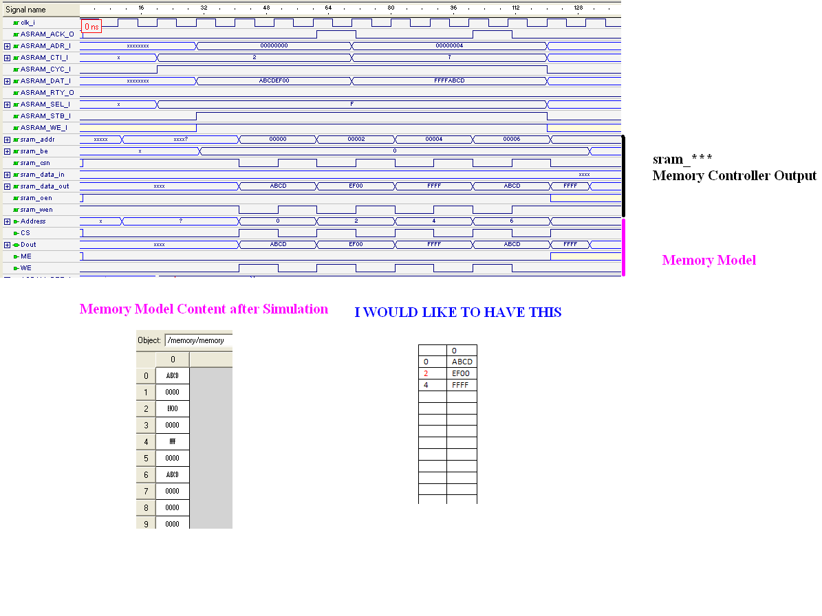
I appreciate your contribution..

In order to get a better understanding of my purpose please just take a
look
at this new grafic which presents the output (Wishbone + Memory
Controller + Memory Model Content) after simulation and then my
question.

Because one picture replaces 1000 words....

I would appreciate any advice before starting with the place/routing
So your Host (wishbone) uses byte addressing und your RAM uses word
addressing.

This is very trivial to adjust, just connect the address lines like
this:

WB A1 -> RAM A0
WB A2 -> RAM A1
...
Angehängte Dateien:
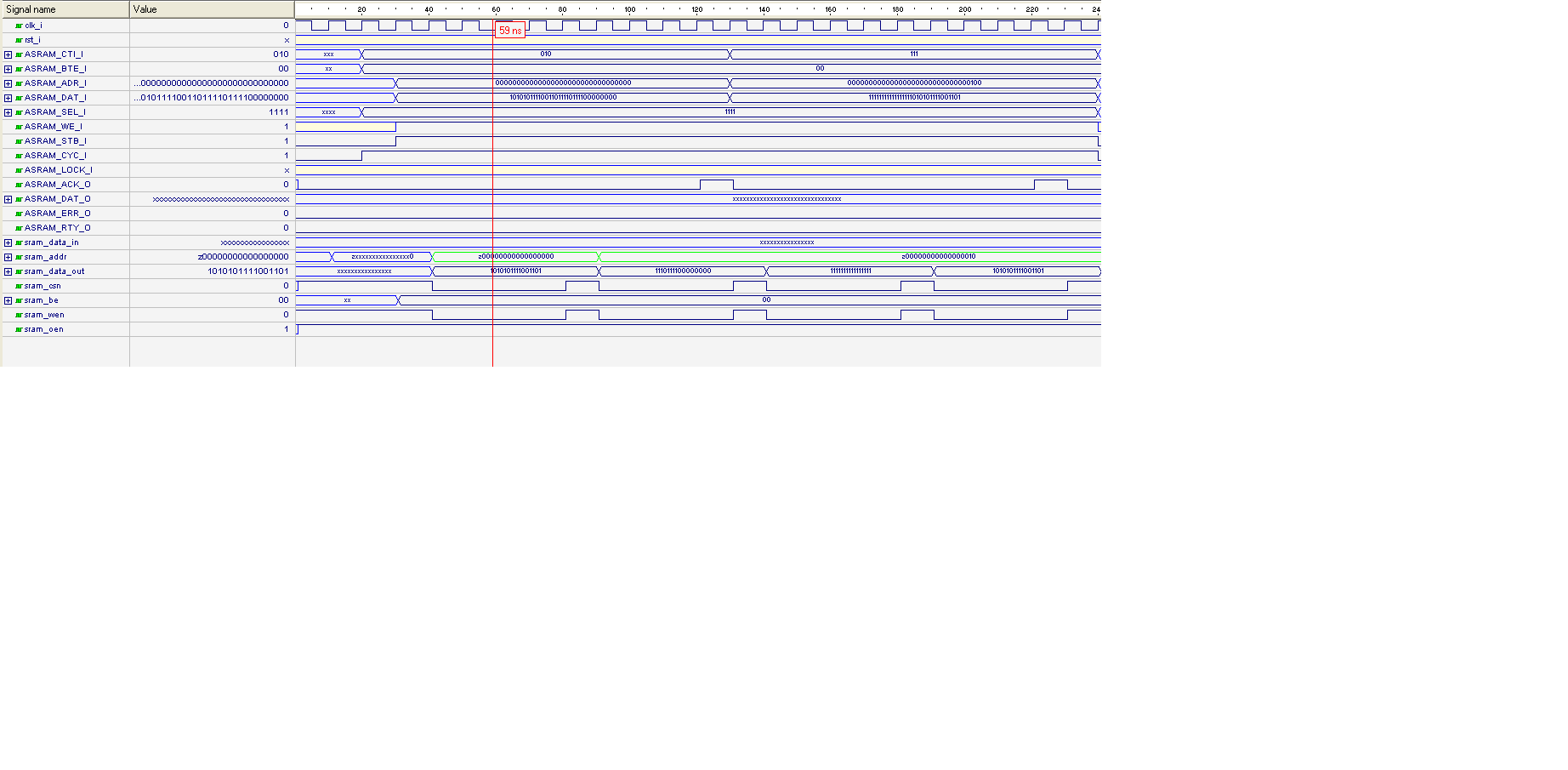
Sorry unfortunately it didn't help me instead it complicated the
simulation output by inserting the following in the instanciation:
.......
 .sram_addr           (WishSRAM_ADR[17:1]),

just take a look
Easy again, the simulation tells you that the highest address bit is
undriven!

You don't have a problem with the SRAM Model, you have a problem with
your whole system design and i am sorry to say, you seem to lack very
basic understanding of system architecture.
Bitte melde dich an um einen Beitrag zu schreiben. Anmeldung ist kostenlos und dauert nur eine Minute.
Bestehender Account
Schon ein Account bei Google/GoogleMail? Keine Anmeldung erforderlich!
Mit Google-Account einloggen
Mit Google-Account einloggen
Noch kein Account? Hier anmelden.