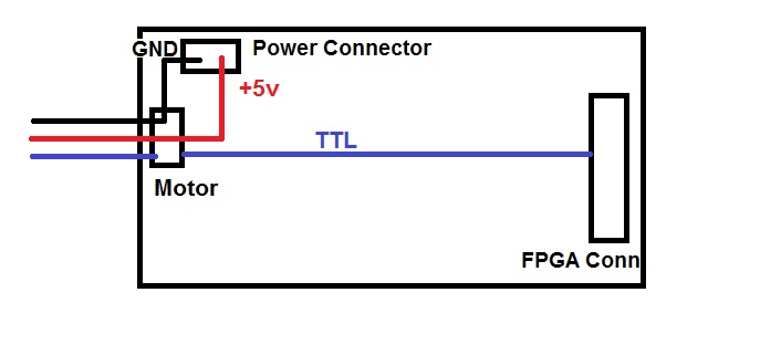
Hello guys!

I need to supply a noise DC motor using +5v of my sensor board PCB. I am
using GND plane and +5v plane to in the PCB and I am afraid that the
noise effect of this motor affect to these power planes or other
components of the sensor board.

My question is of anybody knows about pcb layout technique to isolated
the signals of the motor and its power supply? Maybe should I use some
kind of AO to isolate or any other idea?

Find attach a picture of the PCB.
Angehängte Dateien:
-

PCB.jpg
26 KB
Block most of the noise directly at the motor (M)
1 | +--47uH--+---+---+ |
2 | | | | | |
3 | | | 47nF | |
4 | ----------------+ | | | |
5 | twisted wire 47nF +--(M) |
6 | ----------------+ | | | |
7 | | | 47nF | |
8 | | | | | |
9 | +--47uH--+---+---+ |
Buffer the supply at the connector using an electrolytic. Remember that
a DC motor delivers voltage if braked, and if there is no one to take
the braking power, the voltage rises.

Grab the FPGA VCC from the electrolytic using a choke and following
electrolytic but use no choke in the GND connection.

Does your motor always run ? The is no motor control (full bridge or
MOSFET) drawn.

If you isolate (optocoupler) you may also block GND to the FPGA using a
choke.
Thanks for your soon answer.

there is not any motor control, only the TTL signal provided by the FGPA
trought a buffer/driver. The motor is always running.

On the other hand, having a look to your block diagram is not clear
where should I place the 47nF caps. I have a PCB with a connector with 3
pins. TTL, +5V and GND. Which components should I place in that
connector and how to do it?

The FPGA is in other designed board, so all the solutions to remove the
motor noise should be implemented in the Sensorboard PCB attached in the
first post...So I don´t know if the solution of the choke in the FPGA
side is valid anymore..

Thanks again for the answer!
Bitte melde dich an um einen Beitrag zu schreiben. Anmeldung ist kostenlos und dauert nur eine Minute.
Bestehender Account
Schon ein Account bei Google/GoogleMail? Keine Anmeldung erforderlich!
Mit Google-Account einloggen
Mit Google-Account einloggen
Noch kein Account? Hier anmelden.