1 | void ADC_Init(){
|
2 |
|
3 | /*
|
4 | * Maximum possible ADC frequency = 36MHz, Typical 30MHz
|
5 | * APB2 Clock prescaler = 2, F_CPU = 168MHz --> APB2_CLK = 84MHz
|
6 | * 84MHz / 4 = 21 MHz < 30MHz
|
7 | */
|
8 | // change prescaler to not exceed 30MHz
|
9 | ADC->CCR |= ADC_CLOCKPRESCALER_PCLK_DIV4; // clock divider for all ADC's
|
10 | //ADC1->CR2 |= ADC_CLOCKPRESCALER_PCLK_DIV4; // Clock divider same as Timer divider
|
11 |
|
12 | //enable the ADC Clock
|
13 | RCC->APB2ENR |= RCC_APB2ENR_ADC1EN;
|
14 | //enable the GPIO port C (Pin_C4) CLK
|
15 | RCC->APB1ENR |= RCC_AHB1ENR_GPIOCEN;
|
16 | //enable the DMA1 Controller clock
|
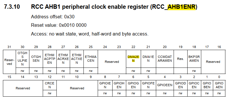
17 | RCC->APB1ENR |= RCC_AHB1ENR_DMA2EN;
|
18 |
|
19 | //configure GPIO as analog input
|
20 | GPIOC->MODER |= GPIO_MODER_MODE4_0 | GPIO_MODER_MODE4_1; // set bit 0 & 1 to high --> 11 = analog input
|
21 |
|
22 | // 10bit Resolution should be sufficient enough. Means a conversion rate 13 ADCCLK cycles (3+10bit)
|
23 | //sampling at Channel IN14
|
24 | ADC1->CR1 |= ADC_RESOLUTION10b; // Set resolution to 10bit.
|
25 |
|
26 | ADC1->SMPR1 |= ADC_SMPR1_SMP14_1; // set bit 1 to high --> 28 cycles per conversion
|
27 | // 28+13 ADC_CLK-cycles/conversion = 41/21MHz = 1.95us / sample. --> 1.95us * 48000 samples = 93.7ms / complete sample block#
|
28 | // --> equals 10 FPS TFT updating-rate (if the FFT is as fast as the ADC conversion)
|
29 | // 30Hz shall be the lowest FFT frequency --> 30Hz/10FPS = 3 times sampling of the lowest frequency --> Nyquist approved
|
30 |
|
31 | //even without using the scan mode, we need to set a "sequence" so the CPU knows which ADC Channel we want to MUX
|
32 | // SQ1 = which channel do we want to measure at first in the sequence, SQ2 would mean which channel as second
|
33 | // Bit 1,2,3 = 01110b = 14 i.e. CHANNEL 14
|
34 | ADC1->SQR3 |= ADC_SQR3_SQ1_1 | ADC_SQR3_SQ1_2 | ADC_SQR3_SQ1_3;
|
35 |
|
36 | //enable ADC and set it to continous mode
|
37 | ADC1->CR2 |= ADC_CR2_CONT | ADC_CR2_ADON;
|
38 |
|
39 | //wait power up time minimum of t_Stab = 2-3us
|
40 | HAL_Delay(1);
|
41 | //run calibration
|
42 | ADC1->CR2 |= 1 << 3; /* Initialize calibration registers */
|
43 | while (ADC1->CR2 & (1 << 3)); /* Wait for initialization to finish */
|
44 | ADC1->CR2 |= 1 << 2; /* Start calibration */
|
45 | while (ADC1->CR2 & (1 << 2)); /* Wait for calibration to finish */
|
46 | ADC1->CR2 |= 1 << 22; /* Start first conversion */
|
47 |
|
48 | /* DMA Settings */
|
49 |
|
50 | DMA2_Stream0->PAR |= (uint32_t)(&(ADC1->DR)); // Base address of the peripheral data register from which the data will be read
|
51 | DMA2_Stream0->M0AR |= (uint32_t)&ADC_value; // Base address of Memory area 0 to which the data will be written.
|
52 | DMA2_Stream0->NDTR |= 2; // Number of data items to transfer
|
53 | DMA2_Stream0->CR |= DMA_SxCR_CIRC | DMA_SxCR_MINC | DMA_SxCR_MSIZE_0 | DMA_SxCR_PSIZE_0; // enable circular mode, Memory Size 01 --> 16bit, Peripheral Size 01 --> 16bit
|
54 | DMA2_Stream0->CR |= DMA_SxCR_EN; // enable the now fully set up DMA controller
|
55 |
|
56 | ADC1->CR2 |= ADC_CR2_DDS; // enabling a new DMA request after a completed ADC conversion
|
57 | ADC1->CR2 |= ADC_CR2_DMA; // activate the DMA1 controller specifically for the ADC1
|
58 |
|
59 | ADC1->CR2 |= ADC_CR2_SWSTART; /* Start first conversion */
|
60 | }
|