1 | // STM32F303 bare bone DMA DAC
|
2 | // create a sin wave table an move the values via DMA to the DAC
|
3 |
|
4 | // https://vivonomicon.com/2019/07/05/bare-metal-stm32-programming-part-9-dma-megamix/
|
5 |
|
6 | uint16_t Frequency = 100;
|
7 |
|
8 | const size_t SINE_SAMPLES = 1024;
|
9 |
|
10 | uint32_t SINE_WAVE[SINE_SAMPLES];
|
11 |
|
12 | void initializeSineTable()
|
13 | {
|
14 | float amplitude = 0.8;
|
15 | for (int n = 0; n < SINE_SAMPLES; n++)
|
16 | {
|
17 | uint32_t x= sin(n * 2 * PI / SINE_SAMPLES) * amplitude * 2047 + 2048;
|
18 | uint32_t y= cos(n * 2 * PI / SINE_SAMPLES) * amplitude * 2047 + 2048;
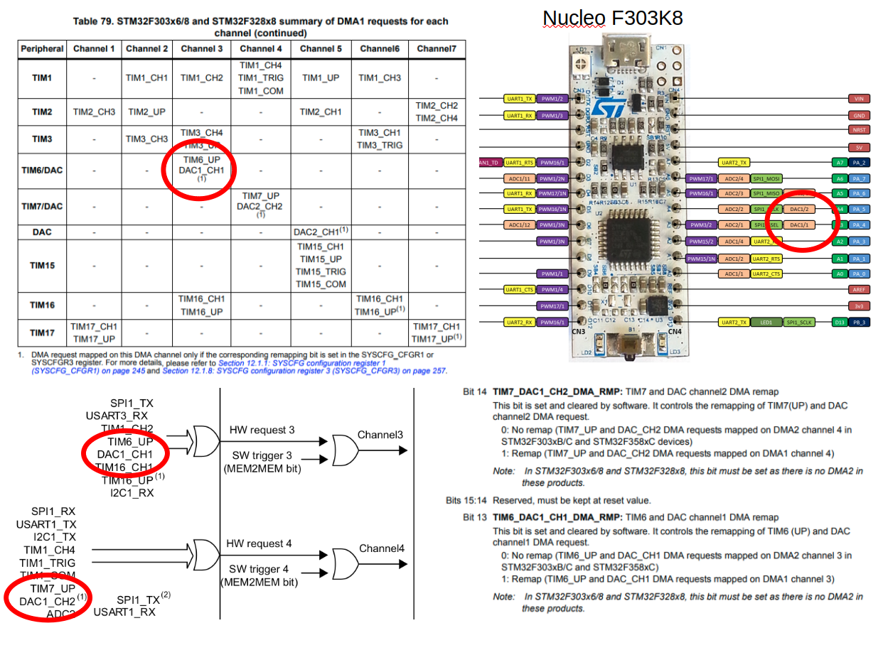
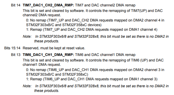
|
19 | SINE_WAVE[n] = x+(y<<16);
|
20 | }
|
21 | }
|
22 |
|
23 | void setDMA_DAC_dualMode()
|
24 | {
|
25 | // Enable peripherals: GPIOA, DMA, DAC, TIM6, SYSCFG.
|
26 | RCC->AHBENR |= ( RCC_AHBENR_GPIOAEN | RCC_AHBENR_DMA1EN );
|
27 | RCC->APB1ENR |= ( RCC_APB1ENR_DAC1EN | RCC_APB1ENR_TIM6EN );
|
28 | RCC->APB2ENR |= RCC_APB2ENR_SYSCFGEN;
|
29 | // Pin A4: analog mode. (PA4 = DAC1, Channel 1)
|
30 | GPIOA->MODER &= ~( 0x3 << ( 4 * 2 ) );
|
31 | GPIOA->MODER |= ( 0x3 << ( 4 * 2 ) );
|
32 | // Pin A5: analog mode. (PA5 = DAC1, Channel 2)
|
33 | GPIOA->MODER &= ~( 0x3 << ( 5 * 2 ) );
|
34 | GPIOA->MODER |= ( 0x3 << ( 5 * 2 ) );
|
35 | // Set the 'TIM6/DAC1 remap' bit in SYSCFG_CFGR1,
|
36 | // so that DAC1_Ch1 maps to DMA1_Ch3 instead of DMA2_Ch3.
|
37 | // (Not all STM32F303 chips have a DMA2 peripheral)
|
38 | SYSCFG->CFGR1 |= ( SYSCFG_CFGR1_TIM6DAC1Ch1_DMA_RMP );
|
39 | // DMA configuration (DMA1, channel 3).
|
40 | // CCR register:
|
41 | // - Memory-to-peripheral
|
42 | // - Circular mode enabled.
|
43 | // - Increment memory ptr, don't increment periph ptr.
|
44 | // - 32-bit data size for both source and destination.
|
45 | // - High priority (2/3).
|
46 | DMA1_Channel3->CCR &= ~( DMA_CCR_MEM2MEM |
|
47 | DMA_CCR_PL |
|
48 | DMA_CCR_MSIZE |
|
49 | DMA_CCR_PSIZE |
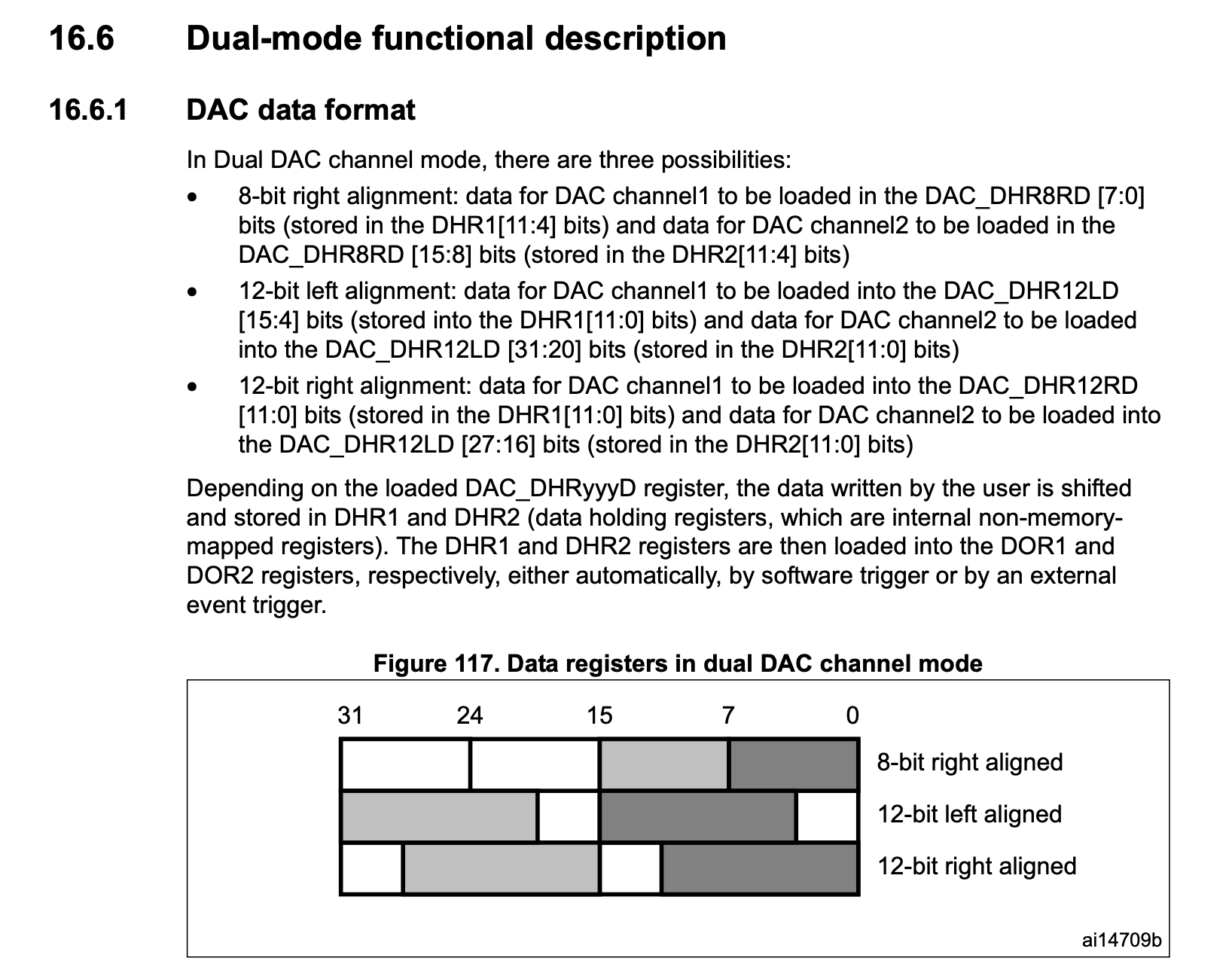
|
50 | DMA_CCR_PINC |
|
51 | DMA_CCR_EN );
|
52 | DMA1_Channel3->CCR |= ( ( 0x2 << DMA_CCR_PL_Pos ) |
|
53 | ( 0x2 << DMA_CCR_MSIZE_Pos ) |
|
54 | ( 0x2 << DMA_CCR_PSIZE_Pos ) |
|
55 | DMA_CCR_MINC |
|
56 | DMA_CCR_CIRC |
|
57 | DMA_CCR_DIR );
|
58 |
|
59 | // Set DMA source and destination addresses.
|
60 | // Source: Address of the sine wave buffer in memory.
|
61 | DMA1_Channel3->CMAR = ( uint32_t )&SINE_WAVE;
|
62 | //obsolete: Dest.: DAC1 Ch1 '12-bit right-aligned data' register.
|
63 | //Dual DAC 12-bit right-aligned data holding register
|
64 | //DMA1_Channel3->CPAR = ( uint32_t ) & ( DAC1->DHR12RD );
|
65 | // Set DMA data transfer length (# of sine wave samples).
|
66 | DMA1_Channel3->CNDTR = ( uint16_t )SINE_SAMPLES;
|
67 |
|
68 | // TIM6 configuration. This timer will set the frequency
|
69 | // at which the DAC peripheral requests DMA transfers.
|
70 | // Set prescaler and autoreload for the frequency
|
71 | TIM6->PSC = ( 0x0000 );
|
72 | TIM6->ARR = ( SystemCoreClock / ( Frequency * SINE_SAMPLES ) );
|
73 | // Enable trigger output on timer update events.
|
74 | TIM6->CR2 &= ~( TIM_CR2_MMS );
|
75 | TIM6->CR2 |= ( 0x2 << TIM_CR2_MMS_Pos );
|
76 | // Start the timer.
|
77 | TIM6->CR1 |= ( TIM_CR1_CEN );
|
78 |
|
79 | // DAC dual mode
|
80 | // https://electronics.stackexchange.com/questions/607624/what-does-dual-dac-mode-mean-for-this-microcontroller-board
|
81 | // Reference Manual RM0316
|
82 | // page 432
|
83 | // DAC configuration.
|
84 | //
|
85 | // *** Simultaneous trigger without wave generation **
|
86 | // To configure the DAC in this conversion mode, the following sequence is required:
|
87 | // 1. Set the two DAC channel trigger enable bits TEN1 and TEN2
|
88 | DAC1->CR |= ( DAC_CR_TEN1 );
|
89 | DAC1->CR |= ( DAC_CR_TEN2 ); // channel 2 trigger enable
|
90 |
|
91 | // 2. Configure the same trigger source for both DAC channels by setting the same value in
|
92 | // the TSEL1[2:0] and TSEL2[2:0] bits
|
93 | // Set trigger sources to TIM6 TRGO (TRiGger Output).
|
94 | DAC1->CR &= ~( DAC_CR_TSEL1 );
|
95 | DAC1->CR &= ~( DAC_CR_TSEL2 ); // channel 2 trigger source the same
|
96 |
|
97 | //3. Load the dual DAC channel data to the desired DHR register (DAC_DHR12RD,
|
98 | // DAC_DHR12LD or DAC_DHR8RD)
|
99 | DMA1_Channel3->CPAR = ( uint32_t ) & ( DAC1->DHR12RD );
|
100 | // Note: the transfer won't actually start here, because
|
101 |
|
102 | //When a trigger arrives, the DHR1 and DHR2 registers are transferred into DAC_DOR1 and
|
103 | //DAC_DOR2, respectively (after three APB clock cycles).
|
104 |
|
105 | // Enable DAC DMA requests for channel 1.
|
106 | DAC1->CR |= ( DAC_CR_DMAEN1 );
|
107 | DAC1->CR |= ( DAC_CR_DMAEN2 );
|
108 | // Enable DAC channel 1.
|
109 | DAC1->CR |= ( DAC_CR_EN1 );
|
110 | DAC1->CR |= ( DAC_CR_EN2 );
|
111 | // Delay briefly to allow sampling to stabilize.
|
112 |
|
113 | delay(10);
|
114 | // the DAC peripheral is not sending DMA requests yet.
|
115 | DMA1_Channel3->CCR |= ( DMA_CCR_EN );
|
116 |
|
117 | }
|
118 |
|
119 | void setup()
|
120 | {
|
121 | initializeSineTable();
|
122 | setDMA_DAC_dualMode();
|
123 |
|
124 | // Done; a low-res 440Hz sine wave should be playing on PA4.
|
125 | Serial.begin(115200);
|
126 | }
|
127 |
|
128 | void loop()
|
129 | {
|
130 | static int n;
|
131 |
|
132 | Serial.print(SINE_WAVE[n]&0xFFFF); Serial.print(' ');Serial.println((SINE_WAVE[n++]>>16)&0xFFFF);
|
133 | if(n>=SINE_SAMPLES)n=0;
|
134 | delay(10);
|
135 | }
|